Polycrystalline silicon substrate
Polycrystalline silicon substrate:
As its name implies, polycrystalline silicon (multicrystalline silicon/ polysilicon) is made up of many small single crystals and is a form of silicon with high purity. So, polycrystalline silicon contains so many grains and also grain boundaries.
Polycrystalline ingots are grown in quartz crucibles which is then cut into square-shaped polycrystalline silicon substrates. Note that the manufacturing cost of solar cell modules includes the cost of silicon substrate (50%), module processing (30%) and cell processing (20%) [1]. As we can see it, the latter costs the least whilst the former costs as much as one half of the total cost. Therefore, the market price is largely determined by the cost of polycrystalline feedstock. This is why reducing the cost of silicon substrate remains one of the biggest changes in the PV industry. Any attempt to reduce the cost of silicon substrates is, in turn, an attempt to reduce the overall cost of solar PV modules and is an effort of expediting the growing share of solar electricity in the energy sector.
The cost of crystalline solar cells is constantly falling.
Anyway…
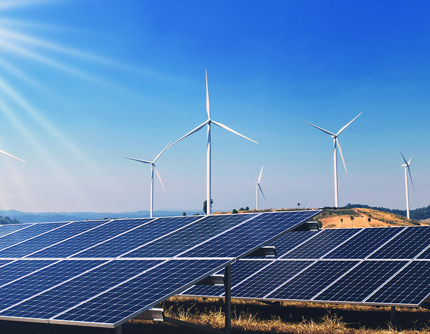
It is worth knowing that both single crystalline and polycrystalline solar PV technologies are already proven, economically viable means of converting solar radiation into electricity.
Doping silicon
High purity silicon is too bad at conducting electricity as it is not a conductor but a semiconductor while the material needed to fabricate solar PVs must show some crucial properties like electrical conductivity. Simply, high purity crystalline is not a good candidate to be used as a light-harvesting semiconductor material in the solar PV industry.
Purity is good. But not here!
But… we are still not unlucky!
Even though high purity crystalline silicon is not originally conducting, we can make it conducting by introducing an insignificant amount of impurities like boron and phosphorus to the high purity crystalline silicon framework. This process is called doping by which extrinsic or doped silicon is formed. Although the amount of impurity is extremely negligible, it impressively improves the electronic, and optical properties needed for the semiconductor industry and plays a vital role in crystalline silicon solar cells.
There are two types of doping: p-type doing & n-type doping. P-type doping is done by introducing dopants with 3 valance electrons such as boron, aluminium and indium. Once they have been integrated into the lattice structure, p-type dopants catch an additional electron creating a hole (lack of an electron) in the valance band of silicon atoms. This increases the hole-concentration and in turn, the conductivity as well since the creation of holes makes the electrons in the valance band mobile. n-type doping is exactly the opposite of p-type doping. It is done by introducing elements with five valance electrons (phosphorous, arsenic, antimony) into the lattice. In this case, each dopant atom contains one more valance electrons than the silicon atoms. Four valance electrons of the dopant atoms combine with four electrons of the outer shell of silicon atoms. The additional electron of the dopant is loosely bounded to the positively charged nuclei and thus free to move and acts as charge carriers. Especially, they require much less amount of photon energy in order to promote to the conduction band (compared to the energy required by intrinsic silicon). This greatly enhances the light-absorbing capacity of the material and thus the efficiency when doped semiconducting material is used to manufacture solar cells.
Reference
[1] Dalapati, G. K., Masudy-Panah, S., Kumar, A., Tan, C. C., Tan, H. R., & Chi, D. (2015). Aluminium alloyed iron-silicide/silicon solar cells: A simple approach for low cost environmental-friendly photovoltaic technology. Scientific reports, 5, 17810.
Ctd